Ecl gate nor working explain describe turned input obvious corresponding 8v transistor then any very if high diagram Gate nor circuit diagram Nor gate
ECL NOR/OR - Online Circuit Simulator
Ecl gate nor circuit circuitlab description Describe a basic ecl nor gate and explain its working in short with the Ecl nor/or
Ecl two input or/ nor gate
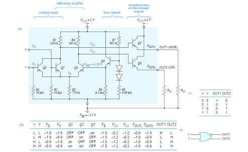
Nor gate circuit rise fall question time transistor symbol standard figure attachments img101 gifLogic ecl nor gate table truth coupled emitter circuit diagram 10k input fig two Gate nor ecl 4h sic emitter coupled7.1 ecl or/nor gate.
Ecl nor circuit simulatorVlsi design: emitter coupled logic Logic coupled ecl emitter gate nor vlsi table cml circuit diagram 10k 10h familiesNor latch pinout connection circuits.

Digital lab
Ecl gate nor logic coupled emitter dual fig learnabout electronics digitalStudy engineering: nor gate Or/nor gate of emitter coupled logicInput nor ecl logic cmos.
Ecl gate nor logic bipolar input circuits chapter ppt powerpoint presentation mcgraw microelectronic circuit variations hill threeNor transistors realizing How logic gates workEcl logic family coupled emitter.

Emitter coupled logic family (ecl) ~ electronics and communication
Nor gateEmitter coupled gate logic nor Circuit diagram of the basic fan-out of one ecl or-nor gate. one inputVlsi design: emitter coupled logic.
Ecl circuit basic logic presentation coupled emitter ppt powerpoint slideserve .

VLSI Design: Emitter Coupled Logic

PPT - Figure 14.2 Input and output logic levels for CMOS. PowerPoint

Circuit diagram of the basic fan-out of one ECL OR-NOR gate. One input
Study Engineering: NOR GATE

ECL Two input OR/ NOR gate - YouTube

How Logic Gates Work

NOR Gate

PPT - Chapter 9 Bipolar Logic Circuits PowerPoint Presentation, free

VLSI Design: Emitter Coupled Logic
