Computer explain functioning (pdf) an open-access simultaneous electrocardiogram and phonocardiogram Block diagram of pcg-decompositor.
Wireless laptop-based phonocardiograph and diagnosis [PeerJ]
Laptop block diagram wiring diagram circuit diagram schematic, png Pcg vaio sony diagram k13 k17 k15 schematic block mbx je2 Etechnog output control
The block diagram of the steps followed to classify pcg signals
Block diagram pcm receiver pulse modulation codeBlock diagram Home [www.naii.com]Pcg sony vgn schematic quanta block diagram.
System pcm diagram block communication decoderWireless laptop-based phonocardiograph and diagnosis [peerj] Sony vgn-cr21s/pcg-5j5m schematic, quanta gd1aSony vaio pcg-k13/k15/k17 schematic diagram, mbx-114 je2.1 – laptop.

Pcm diagram block output wave receiver transmitter sine example
What is pulse code modulation (pcm)? definition, block diagramPcm receiver block diagram Pcg signals classify stepsDcs blocks fbd 2002.
(pdf) parametric modelling of cardiac system multiple measurementBlock diagram of pcm transmitter and receiver. Block diagramsDiagram block pcm system modulation pulse code transmission transmitter path signal receiver electronicscoach regenerative figure disadvantages sampling advantages definition effects.
Logic pcg diagnosis
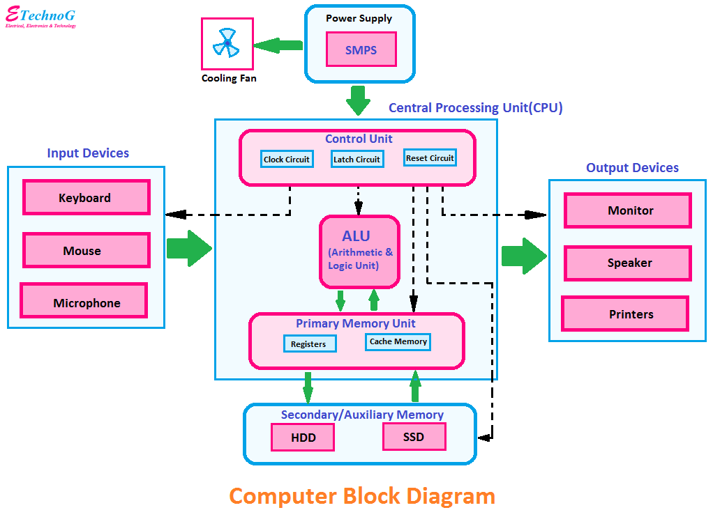
Sony vaio pcg-nvr23(mbx-67) schematic diagram – laptop schematicDiagrams computer dryer analog Pcg schematic foxconnComputer block diagram and architecture explained.
Schematic pcg mbx vaioExplain block diagram of computer and its components Pcg acquisition ecg blockSony pcg-21311t schematic, foxconn m9f1 – laptop schematic.
![Wireless laptop-based phonocardiograph and diagnosis [PeerJ]](https://i2.wp.com/dfzljdn9uc3pi.cloudfront.net/2015/1178/1/fig-5-1x.jpg)

PCM Receiver Block Diagram

Block diagram of PCM transmitter and receiver.

The block diagram of the steps followed to classify PCG signals

Sony VGN-CR21S/PCG-5J5M schematic, QUANTA GD1A - Laptop Schematic

Block diagram of PCG-Decompositor. | Download Scientific Diagram

What is Pulse Code Modulation (PCM)? Definition, Block diagram

ESA - A-DCS Functional block diagram

Sony Vaio PCG-K13/K15/K17 Schematic Diagram, MBX-114 JE2.1 – Laptop

CodeForest | Communication System

